Boost Your Career with Best PCB & Circuit Design Training Course Certification Institute in Noida, Delhi

10+ Years of Excellence in PCB & Circuit Design Training, Courses & Certifications.
Hands on Training on PCB & Circuit Design
Learn from Certified Industry Expert Trainers.
Dedicated placement cell to get you right Job after PCB & Circuit Design Training Course.
Weekday/Weekend Options are Available for PCB & Circuit Design Training Course.
High Quality Best Price PCB & Circuit Design Training, Courses & Certifications by APTRON.
Online Certificate Verification Facility, by APTRON.
International Certificate in Associative with Pearson
Get Free Access To Videos From International Faculties
Placement Support Throw Freshersworld AND Viva Hiring
International Certification Partnership with PEARSON LEARN IT & NETEXPERTS
Enquire for PCB & Circuit Design Training
Price & Details
//

Our Placement & Certification Partners


Placed Students Review


Our Labs Gallarey


PCB & Circuit Design Training, Course, Certification Institute in Noida, Delhi

APTRON is the best PCB & Circuit Design Training institute in Noida that provides the best aws training in noida based on the current industry requirements. PCB & Circuit Design Course in Noida at APTRON has been customized as per the latest developments in the industry and their requirement, which enables the students to get placed in top companies fulfilling their dream of a promising future. APTRON’S PCB & Circuit Design Training in Noida aims at imparting a practical knowledge through live project so that the students acquire professional skills so as to be easily recruited by the top MNCs.

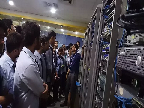
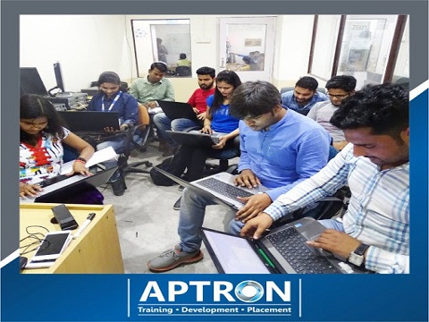
The well-equipped infrastructure and the advanced lab facilities make APTRON the best PCB & Circuit Design Training center in Noida and provides excellent learning environment. PCB & Circuit Design training along with 100% placement assistance makes APTRON one of the most reliable PCB & Circuit Design training institutes in Noida and also the preferred choice for the keen learners. PCB & Circuit Design Training at APTRON is flexible with duration i.e. the classes are conducted everyday, in the evening, at the weekends and also fast-track classes are available for the same. Industry professionals with several years of experience conduct the PCB & Circuit Design training in Noida at APTRON.

APTRON has a dedicated placement team, which is responsible for scheduling of recruitment drives for the students to get placed. Not only this but we also provide a mandatory placement training in order to make the students capable enough to face the interview challenges at the time of recruitment. APTRON’s PCB & Circuit Design course syllabus has been designed in such a way so as to provide both basic and advanced level of PCB & Circuit Design training. APTRON’s PCB & Circuit Design course in Noida has the best PCB & Circuit Design course content that fulfills the requirement of both the beginners as well as the professionals. It has been designed in accordance with the latest developments made and the requirement of the industry.

At APTRON’s well-equipped PCB & Circuit Design training institute in Noida the aspirants learn about started with Amazon cloud, Managing the EC2 infrastructure, Achieving Agility with EC2, Provisioning resources, Storing data in the cloud, Implementing Durable and Reliable Storage, Simplifying the database infrastructure and Amazon Web Services on live projects in addition to the PCB & Circuit Design placement training. The PCB & Circuit Design Training here helps in complete professional transformation of the students in order to achieve their career goals.

About PCB & Circuit Design Course

APTRON’s PCB & Circuit Design training course comprises of the basic understanding of the key concepts, recent trends, and the best practices in order to work with PCB & Circuit Design Architecture. The PCB & Circuit Design training course in Noida at APTRON assists the trainees to develop themselves as industry ready PCB & Circuit Design certified solutions architect and in turn place themselves into top MNCs as a highly qualified PCB & Circuit Design professional.

The PCB & Circuit Design course syllabus covered at APTRON is inclusive of the topics: getting started with Amazon cloud, managing the EC2 infrastructure, Achieving Agility with EC2, Provisioning resources, Storing data in the cloud, Implementing Durable and Reliable Storage, Simplifying the database infrastructure & many more. In addition to this, the institute’s PCB & Circuit Design training in Noida involves practice assignments and real-time PCB & Circuit Design based projects to give the students Hands-on exposure in PCB & Circuit Design management console. Additionally, the PCB & Circuit Design course here helps the aspirants prepare for PCB & Circuit Design Certification exams.

At APTRON PCB & Circuit Design training course duration in Noida is flexible i.e. training classes are conducted in the weekdays and during weekends. APTRON also offers fast-track PCB & Circuit Design training classes in Noida for those running out of time. PCB & Circuit Design course fees here is quite affordable and has been customized as per the trainee’s requirements.

Objective of PCB & Circuit Design Certified Solutions Architect Certification Training

APTRON’s PCB & Circuit Design Certified Solutions Architect Certification Training in Noida aims at helping the learners to:

  • Gain expertise in Enterprise Cloud Solutions Designing and Development via PCB & Circuit Design
  • Migrate Multi-Level Applications to the PCB & Circuit Design Cloud in order to upgrade one’s skill.
  • Learn about Scaling Applications that are Adaptable to Internal Failures as well as High Accessibility
  • Gain proficiency in Designing Resilient and Scalable applications making use of PCB & Circuit Design
  • Qualify the PCB & Circuit Design Certified Solutions Architect – Associate and Professional Level Certification Exams easily.

Why should you go for PCB & Circuit Design Training?

Following are the compelling reasons that make PCB & Circuit Design training course one of the best career choices:

  • Topmost technology in the list of most popular and high paying Jobs across the world
  • More and more companies are opting for Cloud Computing which in turn opens up huge career prospects
  • Certification that Stands as a Proof of your PCB & Circuit Design Skills
  • Be Certified in the fastest Growing Public Cloud services in the world
  • Globally recognized and Acclaimed Certification

Who should take PCB & Circuit Design Training?

Following individuals can take APTRON’s PCB & Circuit Design Certification training in Noida

In order to take PCB & Circuit Design Certified Solutions Architect Associate Certification Training the individuals may be:

  • Absolute beginners or freshers with no prior knowledge about PCB & Circuit Design
  • Aspirants who wish to gain deep insights about PCB & Circuit Design Cloud
  • Any software professional who shows a keen interest in designing and deploying the PCB & Circuit Design based applications
  • Enthusiasts keen on Hosting Fault-Tolerant Applications using WordPress and Joomla on PCB & Circuit Design platform

In order to take PCB & Circuit Design Certified Solutions Architect Professional Certification the individuals may be:

  • Experienced, skilled and expert PCB & Circuit Design Architects
  • Those already certified with PCB & Circuit Design Certified Solutions Architect i.e. Associate Certification

Eligibility / Pre-requisites of PCB & Circuit Design Training

Following is the eligibility required to take APTRON’s PCB & Circuit Design Certification training in Noida

For PCB & Circuit Design Certified Solutions Architect Associate Certification training:

  • The aspirant shall have basic knowledge of Software Programming Principles
  • One should hold basic to Advanced level of expertise on several concepts of Networking and Virtualization

For PCB & Circuit Design Certified Solutions Architect Professional Certification Training:

  • Real-time hands-on experience in the deployment of distributed systems making use of the PCB & Circuit Design Cloud Services
  • Deeper Understanding of PCB & Circuit Design Design Requirements and Best Practices
  • Mandatory PCB & Circuit Design Certified Solutions Architect- Associate Certification

What skills you will learn during PCB & Circuit Design Training?

Following are the skills that you acquire during the PCB & Circuit Design training course in Noida at APTRON:

  • The individuals gain the ability to explain the PCB & Circuit Design cloud and its fundamental structure.
  • One becomes efficient in describing the pricing, account management and pricing. 
  • You explain well about the PCB & Circuit Design cloud values
  • One gets familiar to the basic principles and thus explains well the PCB & Circuit Design Cloud Architecture
  • Gains a better understanding of security, shared security model and compliance concepts.
  • One gains the ability to recognize the major sources of documentation as well as technical assistance. 
  • You get familiar to the main features of deployment and operation in PCB & Circuit Design 

Batch Schedule for PCB & Circuit Design Training in Noida

We provide flexible batch timings to all the students. The PCB & Circuit Design Training Classes in Noida at APTRON is scheduled both in the weekdays as well as weekends in multiple batches during the daytime and evening. However, If the batch doesn’t suit your requirements please let us know. We would try to arrange some appropriate timings depending on your flexibility.

PCB & Circuit Design Certifications

PCB & Circuit Design Certification is a level of Amazon Web Services cloud expertise that the public cloud offers to an IT professional after passing one or more exams. Besides describing an individual’s designing skills, technical skills, and strategic skills, the certification also confirms an individual’s knowledge among the technology into an industry-recognized credential. The certification allows one to gain acknowledgment to his/her technical skills and validate their technical cloud knowledge. Different certification exams are being offered by PCB & Circuit Design for cloud engineers, architects, and administrators. The certification lasts for two years, however, IT professionals are allowed to recertify their certification again. 

Types of PCB & Circuit Design Certification

IT professionals can receive PCB & Circuit Design certification after passing the following certifications based on their profession and interest. In total there are nine PCB & Circuit Design Certifications categorized as associate, professional and specialty level certifications and are recommended on the basis of roles and professional expertise of the individuals, however, the most common ones include:

  1. PCB & Circuit Design Certified Solutions Architect- Associate
  2. PCB & Circuit Design Certified Developer Associate
  3. PCB & Circuit Design Certified SysOps Administrator Associate
  4. PCB & Circuit Design Certified Solutions Architect Professional
  5. PCB & Circuit Design Certified DevOps Engineer Professional
  6. All these PCB & Circuit Design certifications assist the individuals to acquire a better position as well as upgrade their career.

    1. A Foundational PCB & Circuit Design certification for the cloud practitioners with around six months of experience.
    2. Three Associate-level certifications are meant for the professionals withholding experience of a year or more and looking forward to validating and demonstrate their knowledge about the PCB & Circuit Design cloud services (PCB & Circuit Design Certified Developer – Associate, PCB & Circuit Design Certified Solutions Architect –
    3. Three Professional level certifications for individuals with two or more years of experience (PCB & Circuit Design Certified Solutions Architect – Professional and PCB & Circuit Design Certified DevOps Engineer – Professional).
    4. Three Speciality level PCB & Circuit Design Certifications for complex analyses as well as skills related to the cloud services. (PCB & Circuit Design Certified Big Data – Specialty, PCB & Circuit Design Certified Security – Specialty, PCB & Circuit Design Certified Advanced Networking – Specialty)
    5. Amazon Web Services Training in Noida

      APTRON is a trusted name since years when it comes to choosing the best online PCB & Circuit Design training institute in Noida This institute solely aims to provide the best learning experience accompanied with 100% placement assistance to each attendee. Highly experienced trainers with years of Industry expertise conduct the PCB & Circuit Design training classes in Noida, preparing the students into professionals by giving them exposure to the real-time PCB & Circuit Design projects. With a well-equipped infrastructure and highly advanced lab facilities, APTRON is the most preferred PCB & Circuit Design training institutes in Noida for all the keen aspirants. The PCB & Circuit Design course fees here has been customized according to the course content needs of each individual. Additionally, the training here also helps the individuals prepare for various PCB & Circuit Design certification exams. All the aspirant post completion of their PCB & Circuit Design course in Noida get flooded with job opportunities.

      Looking for the best PCB & Circuit Design Certification Training in Noida?

      To know more give us a call, place an inquiry or simply visit our PCB & Circuit Design Training Center in Noida!

      Avail the immense career opportunities that the PCB & Circuit Design certifications offer and without any delay enroll yourself with APTRON’s PCB & Circuit Design online Certification training course in Noida from the industry experts on live PCB & Circuit Design Projects.

The following topics are general guidelines for the content likely to be included on the exam. However, other related topics may also appear on any specific delivery of the exam. To better reflect the contents of the exam and for clarity purposes, the guidelines below may change at any time without notice.

Getting started with Amazon cloud

  • Creating accounts and analyzing the cost breakdown
  • Evaluating Service Level Agreements (SLA)
  • Console, command line tools and API

Overview of the architecture:

  • EC2
  • S3
  • EBS
  • Beanstalk
  • RDS
  • VPC
  • CloudFront
  • SimpleDB
  • SQS
  • CloudWatch

Achieving Agility with EC2:

Managing the EC2 infrastructure:

  • Browsing Amazon Machine Images (AMI)
  • Specifying security groups and key pairs

Provisioning resources:

  • Evaluating Elastic Block Store (EBS) and instance store root devices
  • Assigning elastic IP addresses
  • Mapping instance types to computing needs

Implementing Durable and Reliable Storage:

Storing data in the cloud:

  • Persisting off-instance storage with EBS volumes
  • Creating backups with snapshots
  • Achieving high durability with SimpleStorage Service
  • Transmitting data in/out of the Amazon cloud

Simplifying the database infrastructure:

  • Achieving high availability of nonrelational data with SimpleDB
  • Effortlessly implement a relational database with Relational Database Service (RDS)

Creating cost-effective distributed solutions:

  • Decoupling applications with Simple Queue Service
  • Leveraging CloudFront for high-performance edge cache content delivery
  • Delivering static and streaming content

Adapting EC2 to Your Business Needs:

Customizing virtual machines:

  • Modifying existing images
  • Creating new images off of running instances
  • Converting an instance store AMI to an EBS A

Creating an PCB & Circuit Design cloud architecture:

  • Applying best practices for a cloud solution
  • Selecting a cloud setup for different use case scenarios

Handling Dynamic Resource Requirements:

Monitoring from inside or outside of the cloud:

  • Visualizing utilization metrics with CloudWatch
  • Setting alarms to send and receive notifications

Transparently scaling to meet load variations:

  • Distributing incoming traffic with elastic load balancing
  • Dynamically adding and removing instances with Auto Scaling
  • Setting capacity thresholds

Hosting Applications with Elastic Beanstalk:

Managing application environments:

  • Customizing and configuring platform stacks
  • Provisioning application resources with CloudFormation

PCB & Circuit Design Security Features:

Controlling account security:

  • Configuring access credentials
  • Managing users with Identity Access Management (IAM)

Leveraging the Virtual Private Cloud (VPC):

  • Provisioning isolated PCB & Circuit Design resources
  • Bridging EC2 instances to your internal network with a VPN
  • Launching EC2 instances on dedicated hardware
  • PCB & Circuit Design Training Course is designed according to current IT market.
  • Offer the best PCB & Circuit Design Training Course and Placement with well defined training modules and course sessions.
  • Facilitate regular, weekend and customized PCB & Circuit Design Training Course..
  • One of the biggest team of Certified Expert Trainers with 5 to 15 years of Real Industry Experience.
  • Mentors of PCB & Circuit Design Training helps in major project training, minor project training, live project preparation, interview preparation and job placement support.
  • Smart Labs with Real Latest Equipments.
  • 24x7 Lab Facilities. Students are free to access the labs for unlimited number of hours as per their own preferred timings.
  • Smart classrooms fully equipped with projectors, live racks, Wi-Fi connectivity, Digital Pads.
  • Silent and Discussion Zone areas in Labs to enhance Self Study and Group Discussions.
  • Free of Cost Personality Development sessions including Spoken English, Group Discussions, Mock Interviews, Presentation skills.
  • Free of Cost Personality Development Classes.
  • Hostel Facilities available at Rs 5,500/- month for PCB & Circuit Design Training Course students.
  • Free Study Material, PDFs, Video Trainings, Sample Questions, Exam Preparation, Interview Questions, Lab Guides.
  • Globally Recognized Course Completion Certificate.
  • Extra Time Slots (E.T.S.) for Practical's(Unlimited), Absolutely Free.
  • The ability to retake the class at no-charge as often as desired.
  • One-on-One attention by instructors.
  • Helps students to take knowledge of complex technical concepts.
  • Payment options: Cheque, Cash, Credit Card, Debit card, Net Banking.

About APTRON

10+

Years of Excellence

200+

Routers & Switches Biggest Networking Lab in India
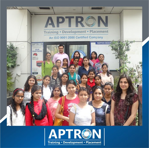
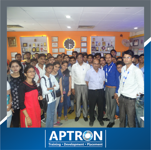
25000+

Students Trained

10000+

Placed Students

Great Career
Program Highlights
Tech-hadoop

No Teacher Only Experts

Industry Expert led training for all.

Tech-hadoop

Training / Practicals / Interview Preparation

Gain practical knowledge of industry.

Tech-hadoop

Globally recognized certification

Join & take your resume to next level.

Tech-hadoop

Life time query support

Through regular forms & query sessions

Tech-hadoop

Weekday/Weekend options

Flexible class timing that suits everyone.

Tech-hadoop

Job Assistance

Dedicated Placement division help you to get a right job.

OUR STUDENT'S REVIEWS
FROM START TO FINISH
SMALL
BATCHES
MENTORING
BY EXPERTS
FLEXIBLE
SCHEDULE
LEARN
BY DOING
GOAL
ORIENTED
TRANSFORM YOUR CAREER WITH APTRON
Enquiry Now
Enquire for PCB & Circuit Design Training
Price & Details
Call Now